Description
The rectifier board has the following roles:
- It converts the alternating current into direct current,
- It selects the best supply voltage for every power supply outputs,
- It limits and measures the current.
The choice to have all these functionalities on one board was motivated by the PCB form factor, the available space in the final LPS box, a logical grouping of these functionalities and the ability to limit the number of interconnections on the power supply lines.
Rectifier
The rectifier board contains the diodes to convert the alternating current into direct current.
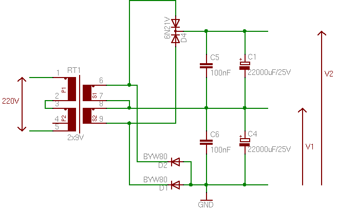
Two 22000uF capacitors are present on each output to produce a steady DC. The DC outputs may vary between 24V and 26V due to the toric transformer. Indeed the toric transformer has an output that could be 10% higher without any load.
<math>18V\times\sqrt{2}-1.6V=23V<math>
Under a maximum load of 4A (thus overloading the transformer) the output voltage swing will be arround 2.6V for the 24V output and 1.3V for the 12V output (at 100Hz).
<math>dV = \frac{i \times 0.007}{C}<math>
Voltage Switch and Filter
At the begining of LPS design, two fixed power supplies of +5V and -5V were defined. In that design, the +5V and -5V were driven by one of the middle voltage produced by the rectifiers (a 9V transformer producing 13V as DV voltage). But it turns out that it was easier to only have several variable power supplies and set them to these low voltages. The 2x9V transformer was kept and a voltage switch was introduced to optimize the power supplies.
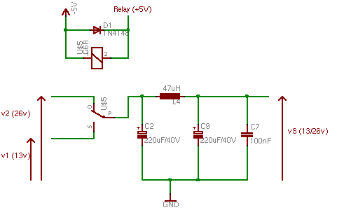
A 1RT relay is used to switch the voltage and select either the +13V or the +26V DV voltage produced by the rectifier (respectively -13V and -26V for the negative supply). When the output supply is below 10V, the relay is activated to select the +13V unregulated DV voltage. This limits the dissipation heat on the power supply transistor. By default the relay selects the +26V. The relay must be capable of supporting currents arround 5A with maximum current of 10A. The OMRON relay G6R and SIEMENS V23061 are specified as 1RT/8A with maximum current on 10A.
The voltage switch is followed by a low pass LC filter. The intent of that filter is to limit and reduce the interactions of different power supplies. During the voltage switch, the LC filter also limits the current and reduces the voltage spikes.
Measuring the current
To measure the output current a resistor is used in the path of the power transistor controlling the output voltage.
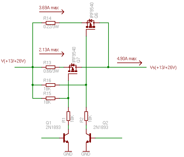
In fact the resistor is composed of two parallel networks composed of a resistor followed by a high power MOSFET transistor. Each MOSFET transistor can be switched on or off. When both are off, the corresponding output voltage is switched off. This feature is used by the protection system controlled by the power supply controller. To compute the current we just need to measure the voltage of the resistor. We must take into account the Rdson of each MOSFET because they are in the current path. The IRF9540 has an Rdson arround 0.117 ohm and some others have an Rdson that can reach 0.48 ohm. In that later case it is possible to remove the resistor to only have two parallel MOSFETs. The table gives the different values of R1 when at least one MOSFET is on.
The MOSFET transistors are controlled by an open drain output provided by the Power Supply Controller. The open drain outputs are implemented by using the Q1 and Q2 NPN transistors (2N1893 because I had many). The MOSFET has a maximum VGS that is arround 20V which is too low since the power supply input voltage can reach 26V. To protect the resistors R1 and R2 are added in the path to limit and make sure the VGS of the switching transistors will remain in acceptable range.
| R1 | Rdson max | I max | V max (Rdson = 0) | V max (Rdson max) |
|---|---|---|---|---|
| 0.66 (3W) | 0.117 | 2.13A | 1.4V | 1.65V |
| 0.22 (3W) | 0.117 | 3.69A | 0.81V | 1.24V |
| 0.165 | 0.117 | 4.90A/5.28A | 0.81V | 1.24V |
Two ways can be used to measure the current or voltage arround R1.
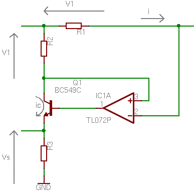
<math>Vs = \frac{R3 \times R1}{R2} \times i<math>
The operational amplifier has its inputs which can range from 0 to the maximum output voltage supported by the power supply. Therefore we must provide it a power supply that is 1 or 2 volts greater than the maximum output voltage.
A second issue more important occurs when the output power supply has a low voltage and high output current. We have a constraint that Vs <Vo. If="" this="" is="" not="" satisfied,="" then="" the="" transistor="" Q1="" cannot="" drive="" the="" current="" in="" R3="" from="" its="" collector.="" Due="" to="" the="" NPN="" transistor,="" the="" current="" that="" flows="" in="" R3="" will="" come="" from="" the="" Q1="" base="" and="" Vs="" will="" grow="" without="" any="" relation="" to="" the="" current="">i.
| R1 | R2 | R3 | i | Vs |
|---|---|---|---|---|
| 0.66 | 2.2K | 15K | 1.2A | 5V |
| 0.165 | 2.2K | 15K | 4.8A | 5.4V |
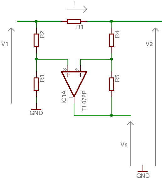
R3 * R1 Vs = ---------- * i R2
The gain created by R3/R2 is chosen to be near 4 to maximize the output voltage swing for the analog converter.
One advantage of the differential solution is that we do not have the limitation or constraint on the output voltage. It also offers a low impedance result due to the operational amplifier output.
Positive vs Negative Board
The positive and negative rectifier boards are very closes but they have small differences:
- The negative board has its ground connected to the highest positive output of the rectifier (hence creating negative outputs).
- The AOP used to measure the current is reversed to take into account the difference in current flow (positive vs negative).
- The AOP uses different supply voltages to produce in both case an output in the range 0..+5V while the inputs have positive or negative values.
- The switching current MOSFET transistors are N-channel for the negative board and P-channel for the positive board.
- Capacitors have their polarity which is reversed.
Connectors
The rectifier board is connected to the power supply microcontroller board for the control and measurement of the output current. For the power distribution it has several one wire high power connectors (not described here). The positive and negative power supply rectifier boards have the same connector.
| POWER_CONTROL | ||||
|---|---|---|---|---|
| 1 | IS11 | MOSFET driver current selector 0.22 ohm (active low) | Power supply 1 | |
| 2 | IS12 | MOSFET driver current selector 0.66 ohm (active low) | ||
| 3 | RE1 | Power supply relay selector (active high) | ||
| 4 | Io1 | Output current measure | ||
| 5 | X | AOP and relay supply | ||
| 6 | -5V | |||
| 7 | gndref | Ground reference for current measurement | ||
| 8 | +24V | AOP using -5V for negative supply (DV = 29V, max = 36V). | ||
| 9 | Io2 | Output current measure | Power supply 2 | |
| 10 | RE2 | Power supply relay selector (active high) | ||
| 11 | IS22 | MOSFET driver current selector 0.66 ohm (active low) | ||
| 12 | IS21 | MOSFET driver current selector 0.22 ohm (active low) | ||
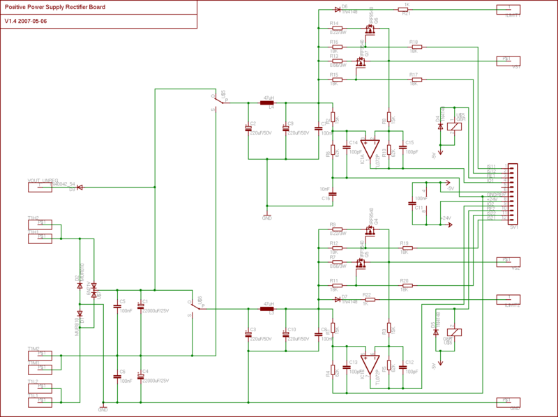
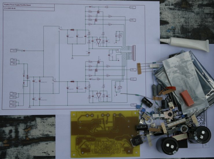
Schematics
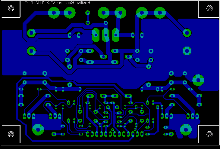
PCB
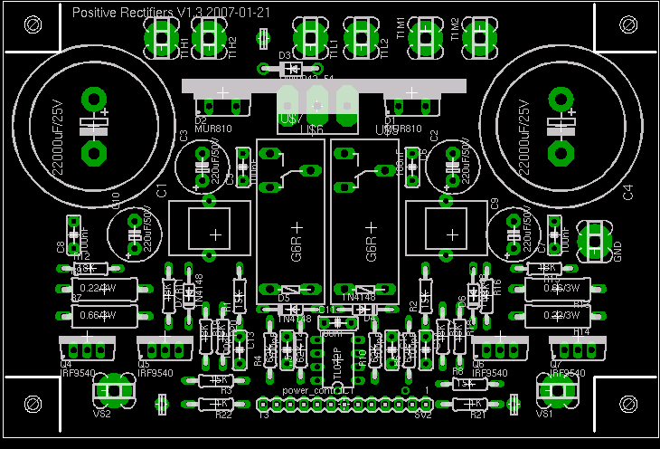
The circuit is made on a 124mm x 83mm PCB using 70um copper. The component placement is such that we can put the positive and negative rectifier board with their components in front of each other with a maximum height of 70mm. This height is limited by the height of the 20000uF capacitors (50mm) and the height of the MOSFET heat sink (20mm).
The board layout is made with the following constraints (DRC checks):
| Signal class | Width | Clearance | Drill |
|---|---|---|---|
| GND | 2mm | 0.4mm | 1mm |
| Power (VSx) | 2mm | 0.4mm | 1mm |
| signal | 0.4mm | 0.4mm | 0.6mm |
| Others | 0.6mm | 0.4mm | 0.8mm |
The auto layout was made with a smaller clearance (0.3mm) and the routing grid of 0.635mm. After a 100% complete auto route, the clearance was increased to 0.4mm and the PCB was fixed by hand. The wire-to-wire clearance was put to 0.5mm and the number of clearance errors reduced to 6 (there are two wires which are at 0.45mm each). The GND, VS1 and VS2 polygon were drawn at the end (otherwise the auto-router skips the routing of these signals!).
Datasheets
Below is a collection of datasheets, white papers and articles related to the parts used in the board.
Resistors
Capacitors
- SOLID POLYMER ALUMINUM CAPACITOR CHIPS IN DC-DC CONVERTER MODULES REDUCE COST AND SIZE AND IMPROVE HIGH-FREQUENCY PERFORMANCE
- CONDUCTIVE POLYMER ALUMINUM SOLID ELECTROLYTIC CAPACITORS
- Electrolytic Capacitor Guide
- EPCOS Electrolytic Aluminium Capacitor (22000uF/25V)
- EPCOS Electrolytic Aluminium Capacitor (22000uF/16V)
Relays
Semiconductors
Others
Changes
{|border="1" |- |2007-07-28 |v1.4.1 |
- Used 0.6mm width for small signals
|- |2007-05-06 |v1.4 |
- Use a 12-pin connector instead of a 13-pin connector
- Added a 10nF capacitor between the ground and the reference ground
|- |2007-01-21 |v1.3 |
- Added a diode followed by a resistor to provide a hardware current protection on the power supply regulator board
|}